ピックアップ

-

記者の眼
オープンソースソフトは何かの節目を迎えているのではないか
-
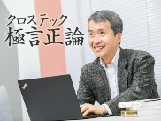
クロステック極言正論
AI時代に勝ち残る条件、あなたは自分の仕事を無くせますか?
-
-
日本大改造
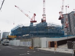
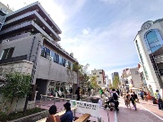
前橋再生の象徴「馬場川通り」、水辺のランドスケープや公衆トイレを民間改修
-

技術者の働き方 ホントの話
自分の仕事はこの先どうなる、不安なときこそ持ちたいもの
-
-

円安で待ったなし!Azureコスト削減法
Azureで知らぬ間に生じる無駄コスト、簡単に監視する仕組みとは
-

世界EV総覧
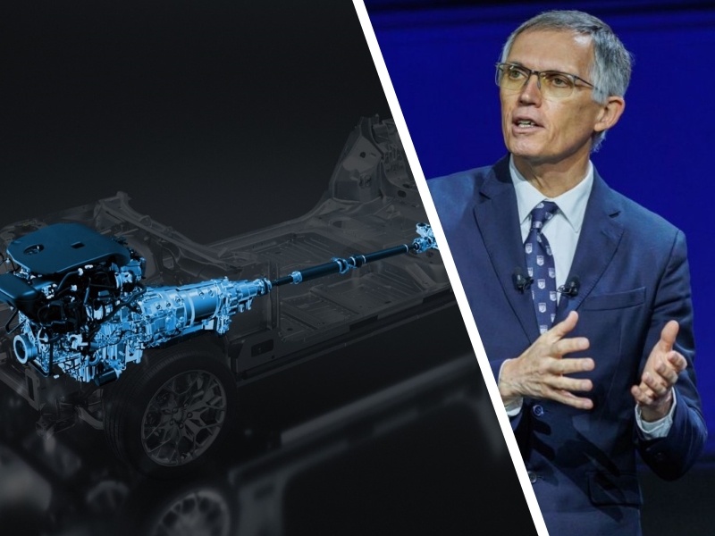
メルセデスのローエンドEV、モデルごとに別方式モーター使うBクラス
-
-

実践DX、SaaSでデータ基盤を構築する「モダンデータスタック」
国産SaaSへの対応が進むETLサービス、Reckoner使いノーコードでデータ連係
-
ニュース解説
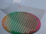
三菱電機がグラフェンで撮像素子を革新、 性能面で一気に飛躍
-
ニュース
-

オラクルが10年で1.2兆円を日本に投資、クラウドとAI領域で
日本オラクルは2024年4月18日、日本での事業に対する投資計画を発表した。クラウドとAI(人工知能)の領域に対し、今後10年間で80億ドル(約1.2兆円)以上を投じる。
-
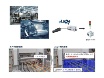
システム計画研究所、画像検査装置に生産設備の監視・点検機能
システム計画研究所(東京・渋谷)は、同社のAI(人工知能)画像検査システム「gLupe(ジールーペ)」に、生産設備の監視や点検を自動化する機能を追加した。少量の画像データを基…
-
奥村組が「肌落ち監視システム」を開発、AIがコンクリートのひび割れを検知
奥村組とシステム計画研究所は「肌落ち監視システム」を開発した。トンネルを掘削した面から岩石などが落下する「肌落ち」の予兆を見つけ出すために、掘削の最先端部分である「切羽(きり…

トピックス
-
日経クロステック編集部おススメ
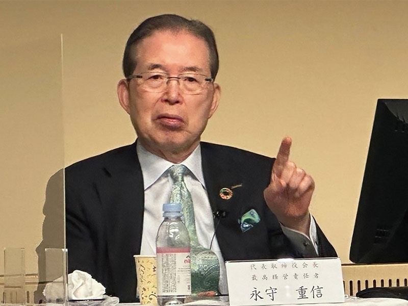
ニデックの新経営体制、世界をどう攻めるか
-
情報技術マンスリー・アーカイブス
IT大手2024年春闘/待ったなし!物流2024年問題/みずほ、なるか4度目の正直
-
先端技術マンスリー・アーカイブス
「EV優先」設計でエンジンに逃げ道/難関だらけのEUV露光装置/寒暖差270℃を耐えたSLIM、月面活動に活路
-
建設業界マンスリー・アーカイブス
日本橋の首都高地下化、大成建設が受注/紀の川ICの変状原因は盛り土の透水性低下/監理技術者の専任緩和へ
-
知ったかぶりをする前に読んでおきたい「IT基本用語辞典」
-
仕事に役立つ! IT・電機・製造・建築・土木の用語集&Excel・Linux・ネットワークのコマンド集
-
ぜひお申し込みください「日経クロステック登録会員(無料)」の特典を紹介
-
有料会員は全記事読み放題!見たい記事が必ず探せる「日経クロステック活用ガイド」
特設サイト


日経クロステック/技術メディアの本
-
図解 木造住宅トラブルワースト20+3 「雨漏り事故」「構造事故」の事例から学ぶ原因と対策
木造住宅のトラブルを「雨漏りワースト20」と「構造ワースト3」として類型化。原因と対策と損害額が...
-
東京大改造2030 都心の景色を変える100の巨大プロジェクト
建築や土木の専門記者が取材した、一歩踏み込んだ東京の再開発プロジェクトを豊富な写真や図面で紹介し...
-
一級建築士矩子と考える危ないデザイン
住宅や建築物で起こる身近な事故と背景、効果的な防止策を人気建築漫画「一級建築士矩子の設計思考」の...
-
ソフトバンク もう一つの顔 成長をけん引する課題解決のプロ集団
ソフトバンクにはモバイルキャリア事業以外のもう一つの顔が存在する。本書ではキーパーソンへのインタ...
-
検証 能登半島地震 首都直下・南海トラフ 巨大地震が今起こったら
地震発生直後に現地で撮影した被害写真を多数掲載。専門家や施設関係者への取材から見えてきた建築・土...
-
次世代自動車2024
【4月30日まで早割実施中!】日経Automotiveが、激動する自動車業界の1年を振り返り、今...


注目のイベント
-
【4月19日】データの活用と保護を両立、「段階的なDX」を実現するIT基盤とは?
2024年 4月 19日 14:00
-
【4月25日】ハイパーバイザーの基本を学ぶ、参加者にはもれなくプレゼント進呈
2024年4月25日(木)
-
プラチナフォーラム 2024 Spring
2024年 4月 26日(金) 13:00~17:00(予定)
-
日経クロステックNEXT 関西 2024
2024年5月16日(木)~5月17日(金)
-
日経ビジネスCEOカウンシル
2024年5月16日(木)17:00~19:50
-
VUCA時代に勝ち残る戦略的サプライチェーン構築に向けて
2024年 5月 24 日(金) 10:00~16:20
-
人手不足を乗り越える 日本の産業界成長のシナリオ2024
2024年5月30日(木)10:20~17:45
-
キャリア・オーナーシップが社会を変える
2024年6月3日(月)~6月5日(水)
-
DX Insight 2024 Summer
2024年6月4日(火)、5日(水)
-
デジタル立国ジャパン2024
2024年6月10日(月)、11日(火)


 注目記事
注目記事


特設サイトアーカイブ


日経クロステック Special
What's New!
IT
- 【生成AI事例】デジタルで現場をDX化
- 業務や役割に応じた「社員に最適なPC」
- 「クラウド時代のあるべき運用」を熱く議論
- 生成AI活用へ「待ったなし」成功の秘訣
- 目指すは相互に行き来できるマルチクラウド
- 「稼ぐ力」を劇的に高めるROIC経営
- 大企業にもキントーンの導入が進む理由
- 「サーバ―」部門満足度トップ企業に訊く
- XDRは「攻めの投資」!運用の三原則とは
- 製造業DX「データドリブン経営成功のシナリオとは」
- 大教大とマウスパソコン教室の在り方を研究
- 欧州トップ企業語る日本のセキュリティー
- NTTドコモ支援の実践型教育プログラム
- 最新の「ポスト認証攻撃」をいかに防ぐか?
- ビジネスPC、ITデバイス購買DXを推進
- ジェイテクトエレクトロニクスのDX事例
- 生成AIの活用の鍵は「内製とアジャイル」
- DXを成功に導くITインフラとは?
- AIと自動化でエンジニアの能力を解き放て
- 最先端のAI技術を支えるNTTPC
- 日本初!東京港を横断する通信網が誕生へ
- NTTデータに優秀なデジタル人財が集まる理由
- 神田れいみと学ぶ「ネットワーク活用白書」
- ゼロトラスト成功の秘訣を神田れいみと探る
- 専門家が斬る日本の意識と対策の現状は?
- 3つのペルソナで、働き方に合わせたPC選び
- オリックス銀行×富士通時田社長 特別鼎談
- ERPプロジェクト≫IT人財の必須条件は
- マネージドサービスが安価に利用できる理由
- 脱レガシー案件≫SIerに必要な人財像は
- DXや生成AI活用に挑む大阪府
- イノベーションの起爆剤
- 3段階で考える、DXで企業力を高める方法
- 大規模プロジェクトでPMが注意すべき点は
- ビジネス戦略と連動したデータマネジメント
- 守りながら攻める“製造DX”の方法論とは
- 最新サーバーに学ぶ熱設計の最前線
- ランサムウエアから診療データはこう守る
- PC管理の課題を課題をまるごと解決
- 日本語に強い「和製生成AIモデル」が誕生
- 動画解説>生成AIからDX変革まで
- 大阪・名古屋エリアのDXが注目される理由
- 最適なネットワークを早く安く簡単に実現!
- セキュリティ×スキルUP≫JSOLの提案
- 力点は「未来予測」へ:データ利活用の勘所
- 生成AI活用でSAP BTPの価値が進化
- ServiceNowでDXを加速≫方法は
- SAPプロジェクトの全体像をいかに描くか
- 先端教育の現場で活躍する大学副学長が使い続けるレッツノート
- 基盤のモダナイゼーションで変革を実現